
AI-generated summary
Lithography, originally an artistic printing technique developed in the late 18th century, has evolved into a cornerstone technology enabling the manufacture of semiconductor chips that power the digital economy. The original method, based on the repulsion between water and fatty substances to transfer images, introduced the critical concept of precisely transferring patterns—a foundational principle that underlies modern chip fabrication. Today, lithography in the semiconductor industry has transformed into photolithography, where light projects intricate patterns onto silicon wafers coated with photosensitive materials. This process is repeated multiple times to build complex, nanometer-scale chip structures, with smaller and more numerous layers enhancing processing power and energy efficiency.
Two main types of lithography dominate the field: Deep Ultraviolet (DUV) and Extreme Ultraviolet (EUV). DUV, operating at a 193-nanometer wavelength, has sustained semiconductor progress for years, while EUV, at 13.5 nanometers, represents a significant technological leap allowing further miniaturization and complexity. ASML, the sole manufacturer of reliable EUV machines, plays a strategic global role, as access to this technology is vital for producing advanced chips essential for artificial intelligence, data centers, and high-performance computing. As semiconductor manufacturing approaches physical and economic limits, emerging techniques like Nanoimprint Lithography and High-NA EUV, along with new materials and 3D architectures, aim to continue enhancing chip capabilities. Lithography thus stands as a critical infrastructure shaping the future of technology, innovation, and geopolitical power.
How lithography enables advanced chips, from their artistic origins to their strategic role in the global semiconductor industry.
Cramming billions of transistors into a space the size of a fingernail is made possible by lithography. This technique makes it possible to manufacture the chips that underpin the digital economy and much of today’s technological innovation.
Although it is at the center of the semiconductor industry today, lithography has a very different origin. It was born as an artistic technique and, over time, it has evolved into an industrial tool of the highest precision.
Walking through that evolution – from the printing shop to the clean room of a chip factory – helps to understand why lithography is a strategic factor in the global technological race.
Traditional lithography: the artistic origin
Lithography emerged at the end of the eighteenth century as a printing technique. It is based on a simple physical principle: water and fatty substances repel each other.
The process involves drawing on a limestone with a fatty material. By wetting the surface, the water is fixed in the areas without drawing. The ink, applied afterwards, adheres only to the drawn areas. This results in an image that can be reproduced with high precision.
This technique had a significant cultural impact. It facilitated the reproduction of illustrations, posters and graphic material, and contributed to the dissemination of knowledge and visual culture.
Beyond its artistic value, lithography introduced a key idea: the ability to transfer precisely defined patterns. That concept – deciding where to act and where not – is the same one that today underpins the manufacture of the chips that make digital technology possible.
Modern lithography: the engine of today’s technology
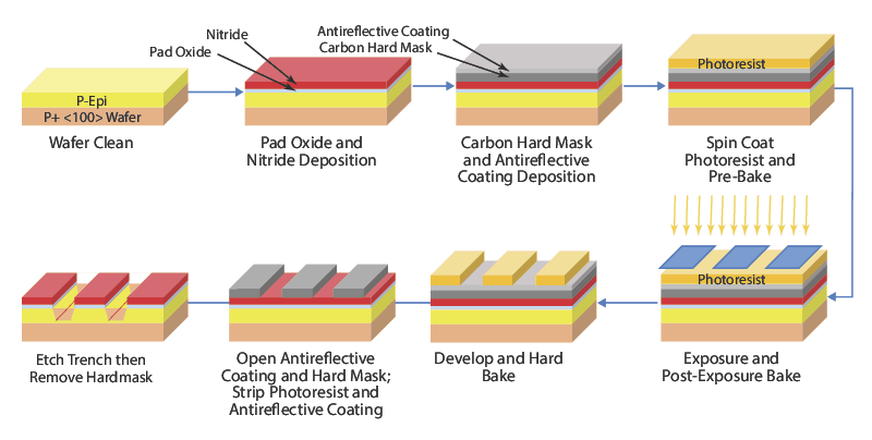
In the semiconductor industry, lithography is evolving into photolithography. The principle is the same as in its origin, but the environment and scale change completely. The stones are replaced by silicon wafers. Manual drawing gives way to light.
The process can be explained simply:
- The silicon wafer is coated with a photosensitive material.
- Light is projected through a mask containing the chip design.
- Light transfers that pattern to the surface.
- Exposed or unexposed areas are eliminated, depending on the type of process.
- The cycle repeats itself dozens of times.
Each repetition adds a new layer of transistors, connections, and logic. The result is an extremely complex structure built at the nanometer scale. The greater the number of layers and the smaller the size of each element, the greater the processing capacity and the better energy efficiency.
Lithography types: DUV and EUV
The miniaturization of chips depends on the ability to transfer smaller and smaller patterns onto silicon. In practice, this translates into the type of lithography the industry uses.
For years, the standard has been DUV (Deep Ultraviolet) lithography. It works with a wavelength of 193 nanometers and has made it possible to sustain the continuous advancement of semiconductors for several technological generations. To this day it is still essential, as it is used in many of the layers that make up an advanced chip.
The next step is EUV (Extreme Ultraviolet) lithography, which operates at a wavelength of 13.5 nanometers. This reduction makes it possible to define smaller structures more precisely and simplify some of the processes required to manufacture them. Thanks to the EUV, the industry can continue to move towards smaller and smaller technological nodes.
The EUV represents a technological leap of great magnitude. Its development requires extreme conditions, such as working in almost absolute vacuum and using optical systems of unprecedented precision. The necessary equipment concentrates decades of research and reaches very high costs, which makes this technology one of the greatest industrial challenges today.
The introduction of EUV marks a turning point in the evolution of semiconductors. It allows the miniaturization of chips to be prolonged and to sustain the increase in computing capacity demanded by the most advanced digital technologies.
The role of ASML
The leap from DUV lithography to EUV has placed ASML in a central position within the global technology ecosystem. The company is the only one capable of designing and manufacturing EUV lithography machines that operate reliably on an industrial scale.
Each of these systems integrates more than 100,000 components and concentrates decades of research in optics, materials physics, software and precision systems. Their technical complexity and cost significantly raise the barriers to entry in the manufacture of advanced chips.
Reliance on this technology has direct implications. The most advanced semiconductors, needed for artificial intelligence, data centers, or high-performance computing, require EUV lithography. For this reason, the ability to access these machines has become a strategic factor for countries and regions.
The concentration of this technological capability in a single vendor has elevated lithography to the rank of critical infrastructure. Access to EUV conditions the production of advanced semiconductors and has become a central element of the global technological and economic balance.
The Physical Limit: Moore’s Law and Nanometers
For decades, the advancement of semiconductors has been guided by a well-known rule of thumb: double the number of transistors on a chip approximately every two years. This sustained progress has been made possible by continuous advances in lithography.
Today, when talking about 5, 3 or 2 nanometer chips, the reference goes beyond size. These technology nodes reflect an increasingly complex balance between transistor density, power consumption, performance, and manufacturing cost.
As the scale is reduced, the challenges multiply. Each new node requires very high investments and coordinated advances in materials, optics, manufacturing processes and design software. The margin for improvement is less and the industrial risk increases.
In this context, lithography is at a critical point. It marks the physical limits of miniaturization, but it also acts as the main lever to continue expanding the computing capacity demanded by advanced digital technologies.
Differences Between Lithography, Engraving and Screen Printing
To better understand the specific role of lithography in this process, it is useful to clarify its relationship with other common industrial methods. In the field of chip manufacturing, it is important to distinguish between processes that, although related, fulfill very different functions:
- Lithography: defines the pattern that you want to reproduce on the silicon through the use of light. This is the step in which the geometry of the chip is established.
- Engraving: Removes material following that pattern. It transforms the design defined by lithography into a physical structure.
- Screen printing: deposits ink through a mesh. It is a printing technique widely used in other contexts, but it has no application at the nanometer scale demanded by the semiconductor industry.
In chip manufacturing, lithography fixes the plane. Engraving makes it a reality.
Source: Semiconductor Etching
The Future: Nanoimprint Lithography (NIL) and Beyond
The EUV lithograph marks the current state of the art, but it does not represent the end point. The industry is already exploring new avenues to further advance chip miniaturization and efficiency.
Among the most relevant lines of research are:
- Nanoimprint Lithography (NIL): Uses physical molds to “seal” patterns directly onto the wafer. This approach reduces dependence on optics and opens the door to potentially simpler and more efficient processes for certain applications.
- High-NA EUV: An evolution of today’s EUV that incorporates even more precise optical systems. Their goal is to further reduce the size of structures beyond 2 nanometers.
- New materials and 3D architectures: miniaturization is no longer advancing only in two dimensions. The vertical integration of components and the use of alternative materials allow capacity to be increased without indefinitely reducing the size.
All these lines share the same objective: to integrate more transistors, reduce energy consumption and expand computing capacity. Lithography will continue to be one of the keys to sustaining technological progress in the coming years.
Lithography: A Critical Infrastructure for the Digital Future
Lithography explains why it is now possible to concentrate enormous computing power on everyday devices. It also helps to understand where the next phase of technological transformation is headed.
In the coming years, the evolution of this technique will be decisive for the development of artificial intelligence, quantum computing, data centers and, in general, for the economic competitiveness of countries and regions. The ability to design and manufacture advanced chips conditions innovation in multiple sectors.
For this reason, lithography is no longer an exclusively industrial matter. It has become a critical infrastructure, closely linked to technological leadership and global balance.
To delve into the strategic role of semiconductors and their impact on the economy and geopolitics, you can consult the Bankinter Innovation Foundation’s Future Trends Forum report on semiconductors:
An in-depth analysis to understand one of the invisible – and decisive – pillars of the digital future.