Enriching the ‘periodic table’ of electronics
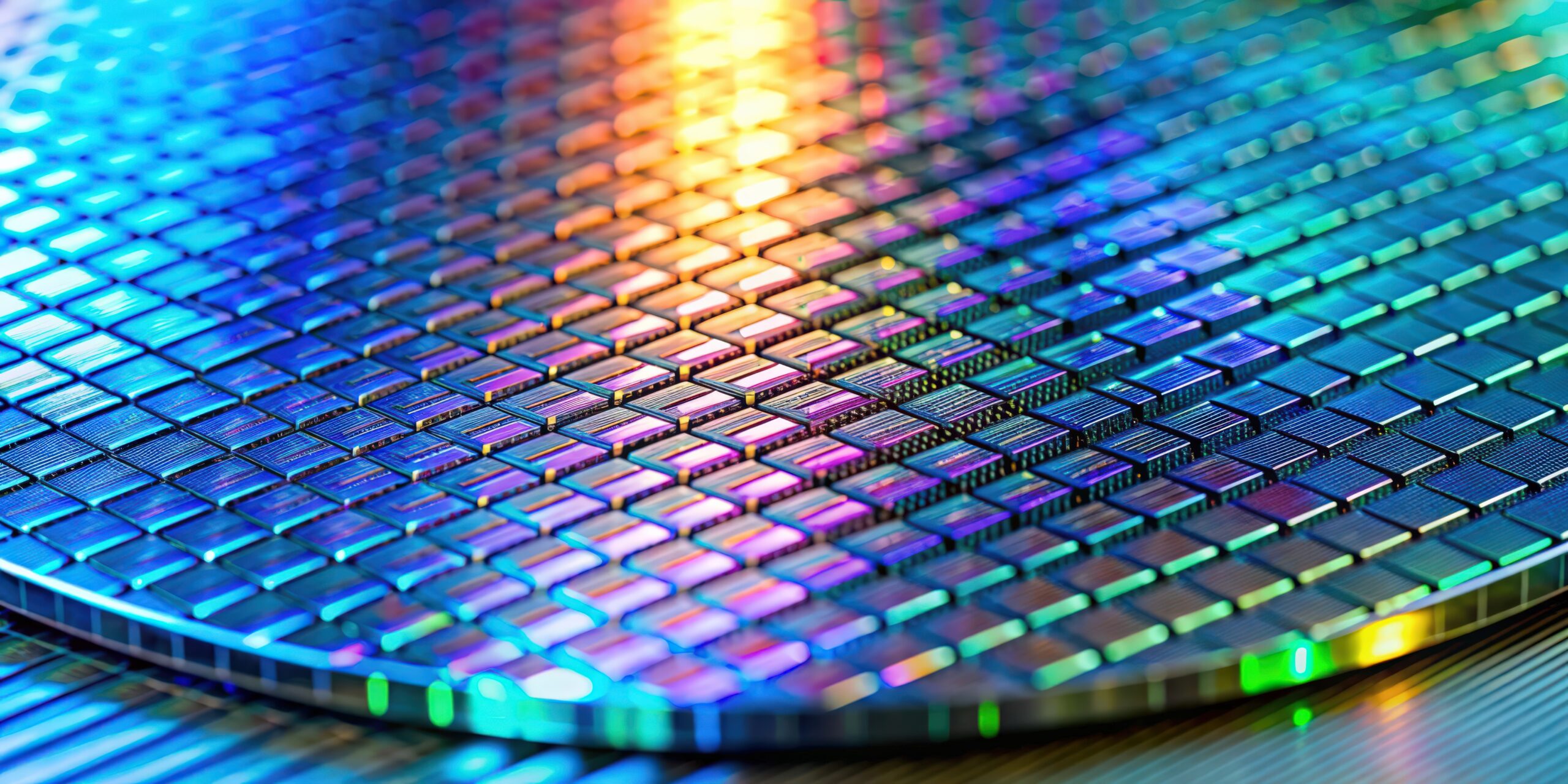
“Semiconductors” today encompasses a diverse set of materials and technologies that extend well beyond silicon, enabling advances along the lines commonly referred to as “More than Moore” (beyond Moore’s Law: non-digital functionalities integrated on chips such as power electronics, RF, sensors, photonics, heterogeneous integration, MEMS, etc.) and “More Moore” (continued Moore scaling: enabling the miniaturization of advanced electronic technology nodes below 2 nm).
Among the most relevant materials are:
• Wide-bandgap semiconductors, such as diamond, silicon carbide (SiC), and gallium nitride (GaN), together with related materials (AlN, AlGaN), as well as emerging materials like wide-bandgap semiconductor oxides, with gallium oxide (Ga₂O₃) as a leading representative. These materials are key to power electronics (fast chargers, inverters, electric mobility) and to applications in extreme environments (high temperature, high-radiation conditions).
• Two-dimensional (2D) materials (such as graphene, molybdenum disulfide (MoS₂), tungsten diselenide (WSe₂), black phosphorus (bP), or hexagonal boron nitride (h-BN)), whose electronic and optical properties can be tuned layer by layer. They hold strong potential for extremely miniaturized transistors and for devices with novel functionalities enabled by interlayer coupling and stacking. In particular, they offer promising applications in neuromorphic devices, photodetectors, single-photon emitters and detectors, and THz modulators. These materials and their heterostructures exhibit exotic physical phenomena that enable, for example, the combination of spintronics with photonics, programmable electronics, or excitonic switches, as well as applications in quantum technologies.
• Topological materials, whether insulators or semimetals, which exhibit electronic properties governed by the topology of their band structure rather than solely by their chemical composition. They host highly robust conducting states at surfaces or edges, protected against defects and disorder, making them strong candidates for ultra-low-dissipation electronics, lossless interconnects, spintronics, quantum computing, and photonic devices. One of the most widely studied paradigms is bismuth selenide (Bi₂Se₃).
• Ferroelectric and phase-change materials, which are fundamental for non-volatile memories and for building artificial synapses in chips that operate in a brain-like manner (neuromorphic computing). Representative examples include germanium–antimony telluride (GST), hafnium oxide, and other oxides such as titanium oxide, strontium titanate, nickel oxide, and certain ternary zinc oxides. Depending on the specific material, properties such as ferroelectricity, memristive behavior, or piezoelectricity can be combined with additional functionalities including photocatalysis, transparent electronics, or specialized sensing, including biosensing.
• Materials for photonics and quantum technologies, required for integrated lasers (III–V compound semiconductors such as indium phosphide, InP), single-photon sources and quantum sensors (based on diamond, SiC, or quantum dots), and integrated photonic circuits (lithium niobate, LiNbO₃). Advanced materials for quantum and photonic technologies are characterized by precise control over their electronic, optical, and quantum properties, enabling efficient manipulation of light and quantum states. Their integration into nanostructures and hybrid heterostructures opens new possibilities for ultrafast, reconfigurable, and energy-efficient devices.
In short, silicon will remain the backbone of the ecosystem, but it is no longer sufficient on its own. Heterogeneous integration will be the key mechanism for incorporating these new materials and for sustaining emerging architectures in advanced computing and electronics.