AI-generated summary
Silicon has been the cornerstone of microelectronics for over fifty years due to its abundance, cost-effectiveness, and excellent electronic properties. However, the semiconductor industry is now facing significant challenges that push silicon to its limits, such as extreme miniaturization, thermal management issues, and increased energy demands driven by sectors like electric vehicles, renewable energy, and telecommunications. As devices become smaller and operate at higher power and temperatures, silicon alone cannot efficiently meet the new performance and reliability requirements. This has prompted a shift toward integrating advanced materials like tungsten, a metal known for its exceptionally high melting point (3,422 ºC) and superior thermal and electrical stability.
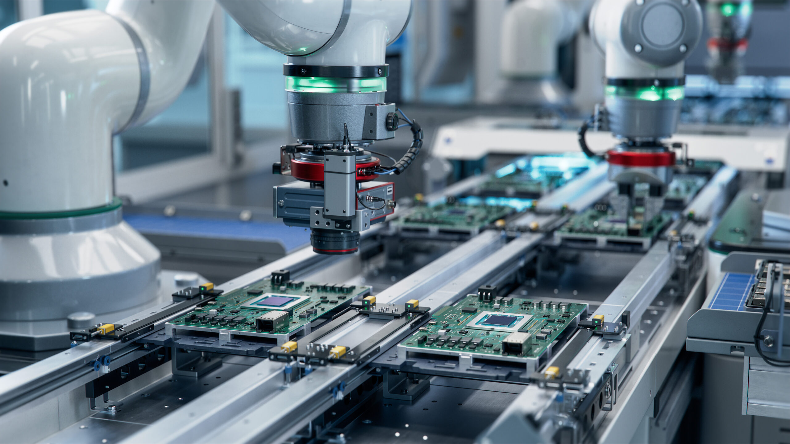
Tungsten plays a crucial but often unseen role inside microchips, especially in the form of tungsten vias—vertical interconnects that link different chip layers. These vias enable more compact, 3D chip architectures capable of withstanding high temperatures and electrical loads, making tungsten essential for power electronics, advanced computing, and next-generation telecommunications like 6G. Its resistance to electromigration and thermal degradation enhances chip durability and efficiency, critical for applications demanding long-term stability. Moreover, tungsten’s strategic importance extends beyond technology; its supply chain, heavily dominated by China, raises concerns about industrial sovereignty and resilience, particularly in Europe. Ensuring secure access and developing comprehensive policies around critical materials like tungsten are vital for sustaining technological leadership and supporting the energy transition in the coming decades.
Tungsten emerges as a key material to overcome the limits of silicon and respond to the new energy demands of advanced electronics.
Silicon [a1] has been the mainstay of microelectronics for more than half a century. However, the industry is beginning to look further. Extreme miniaturization, thermal limits, and increased energy demand are driving the exploration of new materials. In this scenario, tungsten, also known as tungsten (with the chemical symbol W), emerges: the metal with the highest melting point in the world (3,422 ºC) and a key, although not very visible, component of today’s chips.
Tungsten is already part of the microchips we use every day. Their presence is discreet, but essential.
The limitations of silicon: why the industry is looking for new materials
For decades, silicon has been the go-to material on which the entire semiconductor industry has been built. Its abundance, cost and electronic properties have allowed an unprecedented technological scale. However, the current context places demands that go beyond what this material can efficiently offer.
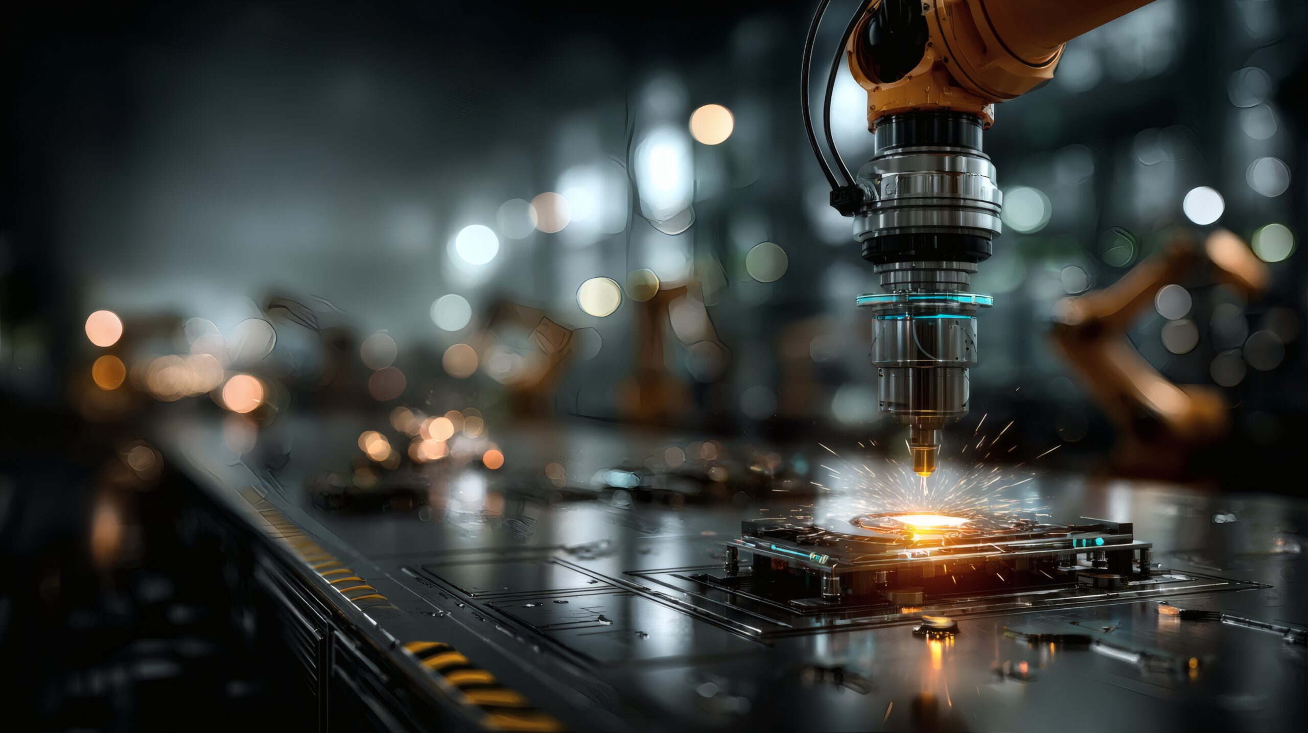
One of the main challenges is thermal management. As devices operate at higher power levels – especially in power electronics and industrial systems – the heat generated becomes a limiting factor. Over-temperature reduces efficiency, accelerates component aging, and compromises long-term reliability.
Added to this is the extreme scaling of technology nodes. The continuous reduction in the size of transistors, which is key to improving performance and reducing consumption, introduces physical phenomena that are difficult to control, such as electrical leakage or degradation of interconnects. These effects are no longer marginal and force us to rethink both the design of the chips and the materials used.
Finally, the electrification of the economy – with the growth of electric vehicles, renewable energies, data centres and smart grids – requires devices capable of operating stably for long periods, under demanding conditions and with high levels of electrical load. In these environments, durability and resistance to thermal and electrical stress take on strategic weight.
As a result, sectors such as electric automotive, energy or telecommunications are driving a transition towards new materials and architectures that allow operating at higher temperatures, managing more power and guaranteeing sustained reliability. Silicon is still fundamental, but the industry is already actively working on its evolution and complementarity with other advanced materials.
The role of tungsten in the new chip architecture
This is one of the least visible – and most decisive – aspects of the current evolution of semiconductors.
Tungsten plays a complementary role to the silicon inside the chip, especially in the internal architecture that allows millions of transistors to be reliably connected. Their contribution is concentrated in the so-called tungsten vias, a key structural element in advanced manufacturing processes.
Tungsten vias serve several critical functions:
- They vertically connect the different layers of the microchip, allowing for increasingly compact and dense designs.
- They support 3D architectures and advanced technology nodes, where vertical integration is essential to further increase performance.
- They provide thermal and electrical stability, even under conditions of high temperature and high current density.
These properties make tungsten a material particularly suitable for environments where long-term reliability is a priority. Compared to other metals used in interconnects, tungsten maintains a predictable behavior under thermal stress and reduces the problems associated with electromigration, one of the great challenges in next-generation chips.
As a result, tungsten has established itself as an essential structural component in power chips and advanced manufacturing nodes. Its role is not visible to the naked eye, but it is decisive for modern architectures to operate at the levels of performance, efficiency and durability demanded by today’s industry.
Sectors that tungsten transforms (where silicon shows its limits)
The impact of tungsten is especially visible in those sectors where electronics operate close to their physical limits. These are environments with high temperatures, high energy flows, and long-term reliability demands. Three areas today concentrate a large part of this transformation.
Electric Automotive (EVs)
The electric vehicle integrates an increasing amount of power electronics. Inverters, fast charging systems and motor control work continuously under high voltages and with significant thermal loads.
In this context, tungsten brings a clear advantage. Its use in the internal interconnects of chips improves electrical and thermal stability, reduces stress degradation and contributes to extending the life of components. This factor is especially relevant in the automotive industry, where reliability and durability have a direct impact on safety and the total cost of the vehicle.
Renewable Energy Smart Grids
Renewable generation systems and advanced power grids rely on electronic devices that operate constantly, often under demanding environmental conditions. Solar inverters, wind converters and grid management equipment require electronics capable of maintaining stable performance for years.
Tungsten strengthens the interconnects of these chips, improves thermal management, and reduces losses associated with continuous operation. Their contribution helps to increase the overall efficiency of the system and reduce maintenance costs, two key factors for the scalability of renewable energies.
6G Telecommunications
The next generation of 6G telecommunications will take electronics to a new level of complexity. Higher frequencies, higher integration density, and increasingly demanding thermal dissipation will shape the design of devices.
In this scenario, tungsten-based interconnects offer a particularly valuable combination of electrical stability and thermal resistance. These properties facilitate the development of chips capable of sustaining the performance required by future networks, where the reliability of the material becomes a strategic element.
Computing: More Power, More Materials
The evolution of computing is moving in several directions at the same time. Artificial intelligence, edge computing , and embedded systems significantly increase the demand for computing power, energy efficiency, and operational reliability. This advance poses challenges that are no longer solved solely by software or algorithms.
As the integration density and power of devices grows, materials become a determining factor. Heat management, electrical stability, and component durability become critical elements to sustain performance in scenarios of intensive and continuous use.
In this context, tungsten plays a discreet but essential role. Its use in interconnects and internal structures allows high-power chips to operate stably under demanding conditions, where other materials show greater limitations. This contribution is especially relevant in advanced computing applications, where the reliability of the hardware directly determines the value generated by the software.
The industry’s trajectory points to a clear conclusion: the future of semiconductors rests on a combination of architecture, design, and advanced materials. Silicon is still the foundation, but computing’s ability to continue scaling increasingly depends on materials capable of accompanying this technological leap.
Technological sovereignty and critical materials: a strategic issue
The debate on semiconductors usually focuses on factories, technological nodes or design capacity. However, the material basis of these devices acquires an increasingly important weight in industrial and geopolitical strategy.
Tungsten is an illustrative example. It is a critical material for the manufacture of advanced chips, with key applications in power electronics, computing, and telecommunications. At the same time, its supply chain is highly concentrated globally. China controls approximately 80–85% of global tungsten production, introducing risks of strategic dependence and geopolitical vulnerability. As its relevance in advanced chips grows, the security of supply of tungsten becomes a key factor of industrial resilience and technological sovereignty.
For Europe, advancing technological sovereignty means looking beyond chip design and comprehensively addressing the entire value chain: from access to critical raw materials to manufacturing, encapsulation and recycling processes. Initiatives such as the European Chips Act point in this direction, but the challenge goes beyond increasing production capacity. It requires a coordinated industrial vision, which integrates advanced materials, R+D, industry and public policies.
This idea connects directly with the reflection of María Marced, an international leader in the sector, who stresses that the chip industry is undergoing a profound transformation and that Europe still has room to position itself, as long as it acts quickly and with strategic ambition. In his speech at the Future Trends Forum on Semiconductors, Marced insists on the importance of strengthening the European industrial ecosystem, reducing critical dependencies and understanding semiconductors as a structural asset for the continent’s competitiveness.
In this context, materials such as tungsten cease to be a technical detail and become a strategic factor. Their availability, processing and efficient use condition Europe’s ability to sustain its energy transition, reindustrialisation and technological leadership in the long term.
The future of semiconductors is played out in laboratories and factories as well as in decisions about supply chains, international cooperation and industrial autonomy. Understanding the role of materials is an essential first step to address this challenge with a systemic and long-term perspective.
[a1]link to silicon article

Expresidente de TSMC Europa