AI-generated summary
Semiconductors have shifted from a background technology to a central strategic asset underpinning AI, data centers, electric vehicles, telecoms, health, energy and defense. The Bankinter Innovation Foundation’s report and webinar series stress that Europe—while possessing strong research, photonics, materials and manufacturing assets—must better concentrate efforts, choose competitive niches, and convert scientific advances into industrial outputs. Key priorities include aligning European demand with industrial commitment, building clusters with critical mass, bridging the “valley of death” from lab to factory, and treating talent as critical infrastructure.
José Bueno (ex-ASML) explained that semiconductors operate on multi-decade roadmaps requiring tight coordination among designers, equipment makers, materials suppliers, software firms and customers. Moving from a lab breakthrough to a reliable, scalable chip involves thousands of processes, massive investments and years of validation—illustrated by ASML’s decades-long development of EUV lithography. Europe’s strength lies in parts of the value chain, but advanced manufacturing remains concentrated in Asia, creating dependencies. Future bottlenecks will include cost, energy, water and, above all, skilled talent. The pragmatic recommendation: Europe and Spain should not try to do everything but must focus on areas with strategic advantage—integrated photonics, AI chip design and specialized foundries—building ecosystems, training talent and sustaining long-term industrial commitments.
In this webinar of the Bankinter Innovation Foundation, José Bueno, former Director of Product Management at ASML, explains how a cutting-edge technology becomes a reliable and scalable industrial product. An informative session on semiconductors, innovation, talent, geopolitics and opportunities for Europe and Spain.
Semiconductors have gone from being a technology almost invisible to the general public to becoming one of the most strategic pieces of the global economy. They are behind artificial intelligence, data centers, the electric car, industrial automation, telecommunications, health, energy, and defense. In other words: a large part of the future competitiveness of companies, industries, and countries will depend on their ability to access, design, manufacture, or integrate increasingly advanced chips.
For this reason, the Bankinter Innovation Foundation has dedicated one of its Future Trends Forum reports to analysing the critical capabilities that Europe must strengthen in order to compete in semiconductors. The report is based on a central idea: Europe has very relevant scientific, technological and industrial assets, but it needs to concentrate them better, choose where it wants to compete and transform knowledge into verifiable industrial results. Its priorities include turning European demand into industrial commitment, competing where Europe can lead, building clusters with critical mass, crossing the “valley of death” between research and industry and treating talent as a critical infrastructure.
As a continuation of this work, the Bankinter Innovation Foundation has started a series of informative webinars to bring this industry closer to a wide audience. In the previous session, Antonio Mesquida helped us understand the global chip value chain, its geopolitical challenges and the opportunities for Europe and Spain in the new geography of semiconductors. That first webinar laid the general map: who designs, who manufactures, who supplies equipment, materials and software, and why artificial intelligence is accelerating a new stage of demand and specialisation.
This new webinar, presented by Marce Cancho, director of the think tank Future Trends Forum, goes a step further. If the previous session explained the global ecosystem, this one focuses on a key question: how does a frontier technology become an industrial product capable of being manufactured with precision, reliability and scale?
To answer it, the Foundation had José Bueno, founder and managing partner of Beclarus Partners Group and previously director of Product Management at ASML, one of the most relevant companies in the global semiconductor chain. José Bueno has worked at Samsung Electronics, in the areas of strategy, planning, sales and marketing within the memory business, and later at ASML, first in corporate strategy and then in product management in the Deep UV business unit.
The session showed the complexity behind each advanced chip: years of planning, frontier technology, specialized suppliers and very demanding industrial execution. And he left a clear idea: for Europe and Spain, semiconductors are not just science; they are industry, talent and competitiveness.
If you want to go into the technical detail, you can watch the full webinar on YouTube. In this article we collect his main ideas.
Watch the webinar here:
Semiconductors: from the technological roadmap to the industrial product
An industry that plans decades ahead
In many industries, talking about three- or five-year planning already implies thinking in the long term. In semiconductors, this horizon may be insufficient.
José Bueno explained that the sector works with technological roadmaps that project the evolution of chips over ten, fifteen or even twenty years. These roadmaps are not simple prediction exercises. They function as instruments for coordination between chip manufacturers, machinery suppliers, research centers, materials companies, software companies, and large industrial customers.
The reason is simple: no company can move forward in this industry alone. Each new generation of chips requires many players to evolve at the same time. If a manufacturer wants to produce more advanced chips, it needs machines capable of making them, compatible materials, proper design software, accurate measurement systems, and suppliers capable of delivering extremely sophisticated components.
In the webinar, José Bueno showed how organizations such as imec publish technological roadmaps that help guide the evolution of the industry. These maps show where chips could advance in the coming years, although they also reflect the enormous difficulty of meeting the planned deadlines. In some cases, technologies initially planned for a specific date are delayed by several years because the physical, technical and economic challenges are more complex than expected.
The first key idea is clear: the advanced chips we use today began to be prepared many years ago. And the chips that will be relevant in a decade are already being researched now.
From the laboratory to the factory: the most difficult leap
One of the most important insights from the webinar is that in semiconductors, innovation does not end when a technology works in a laboratory. In fact, that’s where one of the most difficult phases begins: turning it into something manufacturable.
José Bueno proposed it as the step “from the technological roadmap to the industrial product”. In other words: how a long-term technological vision is transformed into a machine, a process or a chip that can be produced in a reliable, repeatable and economically viable way.
For a technology to reach a semiconductor factory, it must overcome many barriers. It is not enough to prove that something works once. It must work stably, for thousands of hours, within extremely demanding manufacturing processes and with levels of precision that are very difficult to imagine.
The manufacture of an advanced chip can involve more than a thousand different processes and several months from the time a wafer enters the factory until it is converted into functional chips. In addition, a state-of-the-art factory can require investments of tens of billions of dollars.
In the case of memories, José Bueno explained that manufacturers also work with their own roadmaps to decide how to increase capacity, improve performance and reduce consumption. But even when the goal seems clear, bringing it into production is not easy: each technological leap requires redesigning processes, resolving physical limits and coordinating multiple suppliers for years.
For any entrepreneur, manager or student interested in innovation, this is a fundamental lesson: in deep tech, the distance between a good idea and an industrial product can be enormous. And navigating it requires method, patient investment, specialized talent, customers willing to validate the technology and a great execution discipline.
ASML and the complexity of manufacturing the almost impossible
Much of the webinar relied on the example of ASML, the Dutch company that manufactures some of the most complex and critical machines for the global semiconductor industry.
ASML is especially known for its lithography machines. Simply put, lithography allows you to “draw” tiny structures on silicon wafers that will later become chips. The more advanced the chips, the more precision is needed to perform this process.
José Bueno explained that the leap towards EUV lithography – extreme ultraviolet – required solving extraordinarily difficult physical and technological problems. It was necessary to generate light with very specific characteristics, conduct it within a vacuum environment, use mirrors of extreme flatness and develop new materials and measurement systems. Some of these technologies took decades to reach a truly industrial phase.
The example of ASML shows that industrial innovation is not usually a linear or quick story. EUV technology began to be explored decades ago, requiring multimillion+ investments in R&D, collaboration with customers such as Intel, TSMC and Samsung, strategic acquisitions and many years of improvement before becoming a widely used technology in advanced production.
The semiconductor “technology orchestra”
José Bueno used a very useful image to understand this industry: a technological orchestra.
An advanced chip is not the result of the work of a single company. It is the product of a global ecosystem in which designers, manufacturers, material suppliers, software companies, equipment manufacturers, research centers, universities, measurement companies, integrators and end customers participate.
Each actor plays a part of the score. But for the result to work, everyone must be coordinated.
Research centers such as imec, in Belgium; CEA-Leti, in France; Fraunhofer, in Germany; or ETRI, in South Korea, play a very important role in this orchestra. These organizations help connect advanced research, industrial enterprises, and shared technology roadmaps.
This collaboration does not eliminate competition. On the contrary: semiconductors are one of the most competitive, strategic and protected industries in the world. But precisely because of its complexity, even large competitors need to collaborate with suppliers, customers and technology centres to advance the common border.
For Europe and Spain, this idea is key. It is not enough to finance isolated projects. Dense ecosystems must be built, with stable relationships between science, industry, capital, talent and demand.
Europe: critical strengths, but also dependencies
The webinar connected directly to one of the conclusions of the Future Trends Forum report: Europe has very valuable capabilities, but also important dependencies.
On the one hand, Europe has strengths in manufacturing, research, photonics, power electronics, materials, automotive, industry and applied technologies. ASML is probably the most visible example of a critical European capability in the global semiconductor chain.
On the other hand, Europe does not dominate all links in the value chain. Advanced manufacturing is highly concentrated in Asia, especially in Taiwan and South Korea, and many strategic decisions in the sector are conditioned by technological competition between the United States and China.
José Bueno explained that the industry has gone from a stage dominated by purely technological and commercial logic to a phase in which semiconductors are a tool of geopolitical power. Artificial intelligence has further intensified this strategic dimension.
The conclusion is pragmatic: Europe cannot do everything, but neither can it remain on the sidelines. It must identify the links where it can be differential, strengthen them and turn them into solid industrial positions.
Cost, energy, water and talent: the next bottlenecks
The semiconductor industry is used to living with bottlenecks. For years, one of the most visible has been the ability to manufacture with ever-increasing precision. But José Bueno pointed to other challenges that may gain importance in the coming years.
The first is cost. Advanced factories require gigantic investments. Machines are becoming more complex, processes longer and validation more demanding.
The second is energy. Demand for chips is growing driven by artificial intelligence and data centers, but both manufacturing and intensive computing consume large amounts of energy. Efficiency will become an increasingly strategic factor.
The third is water, a critical resource for many semiconductor factories.
The fourth is talent. The industry needs engineers, physicists, chemists, materials specialists, software experts, industrial profiles, manufacturing technicians, product managers and professionals capable of translating science into business.
At this point, the message for Europe and Spain is especially relevant. Without enough talent, there is no credible semiconductor strategy. And talent is not improvised: it is trained, attracted, retained and connected to real industrial projects.
Q&A: Key Questions from the Public
The session ended with a Q&A session that allowed some of the most relevant topics for Europe, Spain and the global industry to be landed.
Is there a semiconductor cluster in Iberia?
His diagnosis was realistic. Spain does not yet have a large semiconductor cluster comparable to the most consolidated hubs in Europe or Asia. However, there are emerging capacities in different territories: initiatives in Madrid, Catalonia, Galicia, Valencia, the Canary Islands and Malaga, among others. He mentioned areas such as photonics, design of chips for artificial intelligence, metrology, new specialised foundries and projects linked to public-private collaboration.
The possible arrival of a large imec hub in Malaga was pointed out as an element that could contribute to better articulating the ecosystem. Initiatives such as Innofab in Barcelona, photonics capabilities in Galicia and Valencia, chip design companies such as Openchip or Semidynamics, and the role of the SETT as a public instrument to support the growth of technology companies were also mentioned.
The underlying idea is that Spain does not need to try to compete all at once in all segments. It can find opportunities in emerging areas where it already has capabilities and where the value chain is still being configured.
Can a serious competitor to ASML emerge?
One of the most interesting questions from the audience was whether there are alternatives to ASML and when competitors capable of disputing its position in the most advanced technologies could appear.
José Bueno was clear: in EUV and High-NA EUV, ASML’s technological distance from potential competitors is very large. According to his vision, someone who wanted to reach the point where ASML is today could need on the order of 10 to 15 years. And even so, ASML would not stand still during that time.
In less advanced technologies, such as Deep UV, there are other players, including Nikon and Canon in Japan, and Chinese companies such as SMEE, which are working on developing their own capabilities. But in the technologies most critical to advanced manufacturing, competing head-on with ASML is extremely difficult.
José Bueno also mentioned that there are technological alternatives in research, such as other lithography methods based on printing or particle beams. However, he placed them on long-term horizons. His personal view is that, if any of these technologies were to mature, ASML would be more likely to incorporate them into its portfolio through acquisition or integration than to see it become a direct competitor on a large scale.
The conclusion is simple: ASML is not only a leader because it manufactures a specific machine, but because it has built over decades an ecosystem of knowledge, suppliers, patents, customers and industrial experience that is very difficult to replicate.
In addition to ASML, what other bottlenecks are there?
Another question from the audience was what other companies or technologies may become bottlenecks within the ecosystem, leaving aside ASML and TSMC.
José Bueno explained that, depending on how memory architectures and three-dimensional manufacturing evolve, certain etching technologies could become as critical as lithography in some processes. He also pointed to materials as a possible bottleneck, especially if silicon begins to find physical limits and new materials are needed to reduce consumption or better control the behavior of electrons within the chip.
What strategy should Europe follow to gain technological sovereignty?
The audience also asked about the European strategy to gain technological sovereignty in semiconductors.
José Bueno insisted that this is a long-term race. Taiwan, South Korea, Singapore or Malaysia did not build their position in a few years. They did so with decades of investment, specialization, talent and industrial development.
For Europe, the recommendation is not to try to dominate the entire value chain, but to build a solid ecosystem and choose areas where it can provide a lot of value. Among the key elements, he mentioned the training of talent, the growth of specialized companies, the creation of ecosystems around technological hubs and the commitment to emerging technologies in which Europe can position itself soon.
Marce Cancho connected this idea with the Draghi report and with the need to bet on few disruptive technologies, instead of dispersing resources on too many fronts. José Bueno agreed that this approach can be applied to both Europe and Spain.
What opportunities appear in emerging technologies?
Areas such as integrated photonics, chip design for artificial intelligence and other technologies that are still in the growth phase came up in the conversation.
José Bueno pointed out that these segments can offer opportunities because they are not yet completely closed by the large global players. For Spain and Europe, the key would be to enter early, build capabilities, train talent and accompany companies during their growth process.
The idea is not to compete where others are thirty years ahead, but to find the windows where technology is changing and where smart specialisation can become an advantage.
Will flexible organic chips be relevant?
Another question from the audience focused on flexible organic chips. José Bueno acknowledged that he does not have specific direct experience in this technology, but pointed out that they could have applications in areas such as IoT, RFID, logistics, connected clothing, product traceability or low-cost and specific use devices.
Although they would not necessarily compete with the large segments of logic and advanced memory, this type of chip can open up very different markets, more linked to everyday objects, distributed sensors and applications where cost and flexibility are more important than maximum computing power.
The big lesson: competitiveness is built before the market arrives
The webinar with José Bueno leaves a clear idea: in semiconductors, competitive advantage is not improvised.
When a technology reaches the market, many important decisions were made years before: what materials to use, which suppliers to incorporate, what talent to train, what investments to assume and which partners to collaborate with.
For Europe and Spain, the challenge is to better connect the capacities that already exist, choose priorities well and sustain them over time. There are universities, technology centres, start-ups and industrial sectors that can play a relevant role, but continuity and focus are needed.
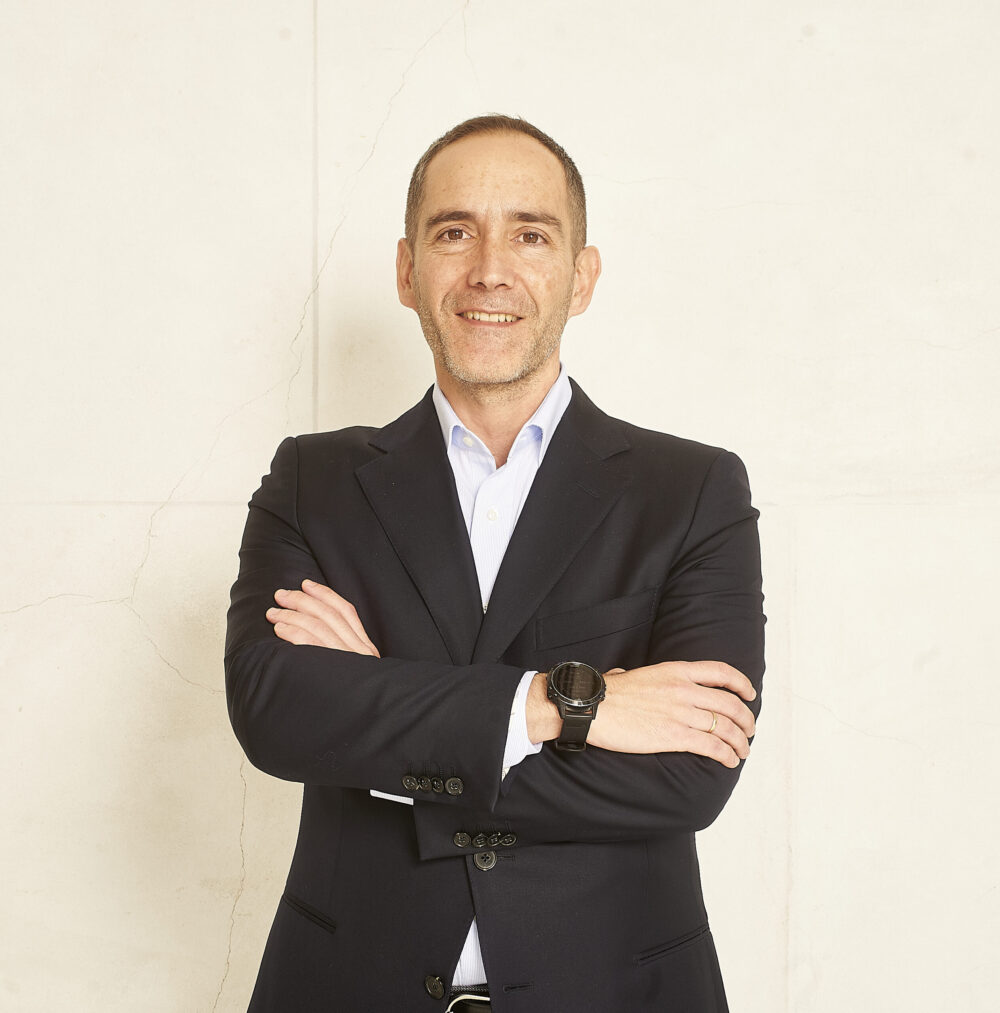
Exdirector de Gestión de Productos en ASML